
Scientists at Johns Hopkins have uncovered a brand new option to construct microchips so small they’re almost invisible.
By combining metals and light-sensitive chemistry, they’ve pioneered a technique that would make chips sooner, cheaper, and much more highly effective. This leap in microchip design might reshape all the things from smartphones to airplanes, opening a path to the following period of know-how.
Breakthrough in Microchip Innovation
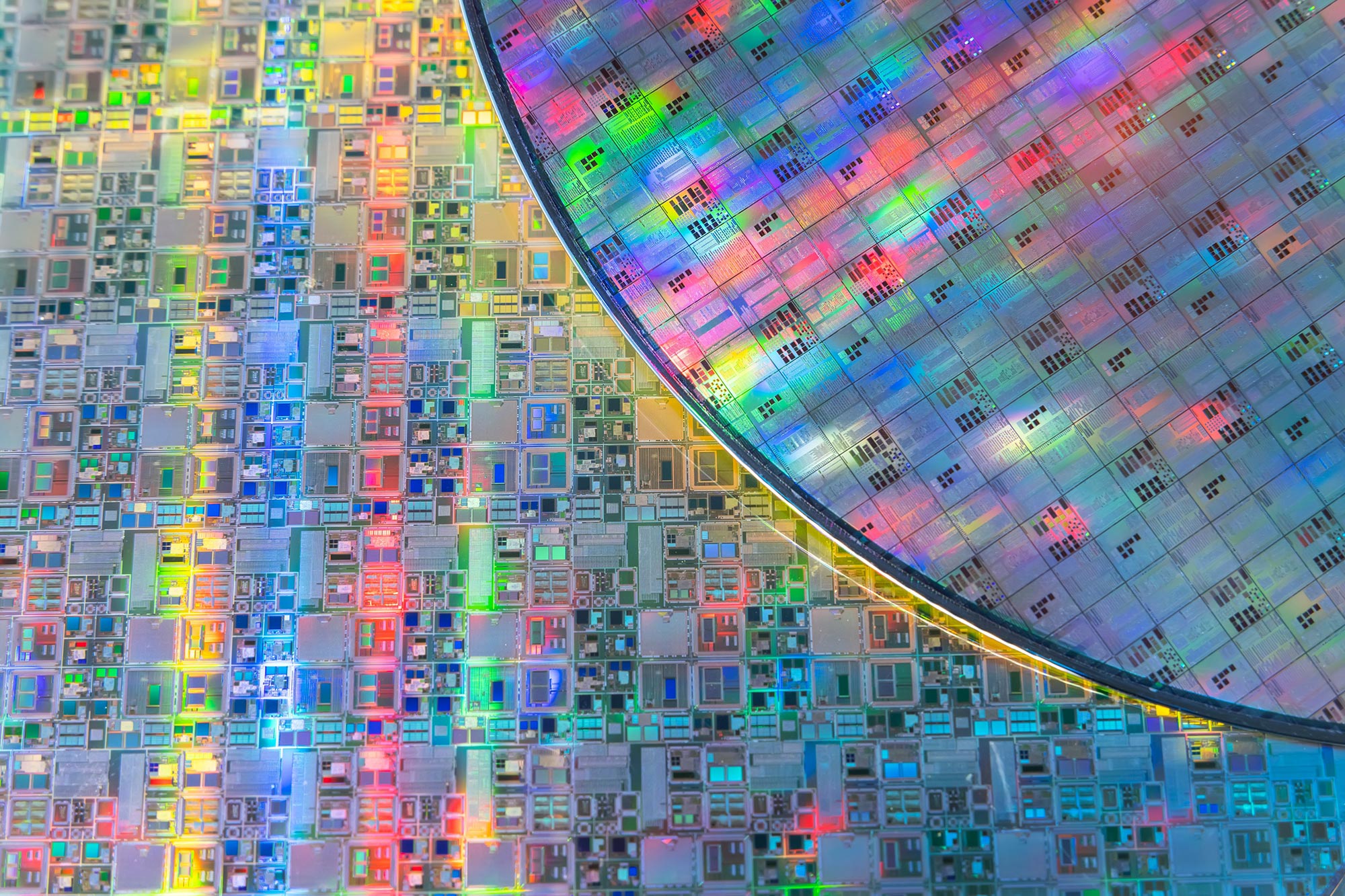
Researchers at Johns Hopkins have recognized new supplies and developed a brand new approach that would speed up the race to supply microchips which can be smaller, sooner, and extra inexpensive. These chips energy almost each nook of contemporary life, from smartphones and family home equipment to cars and plane.
The scientists demonstrated construct circuits so tiny they can’t be seen with the human eye, utilizing a technique designed to be each extremely correct and cost-effective for large-scale manufacturing.
The outcomes of this analysis had been revealed just lately in Nature Chemical Engineering.
Overcoming Manufacturing Boundaries
“Corporations have their roadmaps of the place they wish to be in 10 to twenty years and past,” mentioned Michael Tsapatsis, a Bloomberg Distinguished Professor of chemical and biomolecular engineering at Johns Hopkins College. “One hurdle has been discovering a course of for making smaller options in a manufacturing line the place you irradiate supplies rapidly and with absolute precision to make the method economical.”
In accordance with Tsapatsis, the superior lasers required to etch patterns at these extraordinarily small scales are already obtainable. The lacking piece has been the correct supplies and strategies that may maintain tempo with the demand for ever smaller microchips.
How Microchips Are Made
Microchips are flat items of silicon with imprinted circuitry that execute fundamental capabilities. Throughout manufacturing, producers coat silicon wafers with a radiation-sensitive materials to create a really positive coating known as a “resist.” When a beam of radiation is pointed on the resist, it sparks a chemical response that burns particulars into the wafer, drawing patterns and circuitry.
Nevertheless, the higher-powered radiation beams which can be wanted to carve out ever-smaller particulars on chips don’t work together strongly sufficient with conventional resists.
Pushing Previous Present Limits
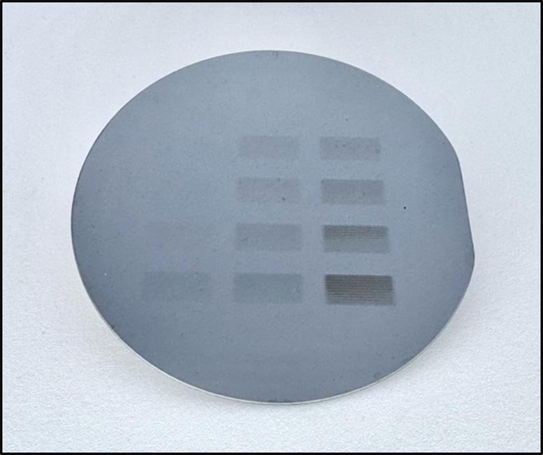
Beforehand, researchers from Tsapatsis’s lab and the Fairbrother Analysis Group at Johns Hopkins discovered that resists made from a brand new class of metal-organics can accommodate that higher-powered radiation course of, known as “past excessive ultraviolet radiation” (B-EUV), which has the potential to make particulars smaller than the present commonplace measurement of 10 nanometers. Metals like zinc take up the B-EUV gentle and generate electrons that trigger chemical transformations wanted to imprint circuit patterns on an natural materials known as imidazole.
This analysis marks one of many first occasions scientists have been in a position to deposit these imidazole-based metal-organic resists from resolution at silicon-wafer scale, controlling their thickness with nanometer precision. To develop the chemistry wanted to coat the silicon wafer with the metal-organic supplies, the crew mixed experiments and fashions from Johns Hopkins College, East China College of Science and Expertise, École Polytechnique Fédérale de Lausanne, Soochow College, Brookhaven Nationwide Laboratory and Lawrence Berkeley Nationwide Laboratory. The brand new methodology, which they name chemical liquid deposition (CLD), will be exactly engineered and lets researchers rapidly discover numerous combos of metals and imidazoles.
“By taking part in with the 2 elements (steel and imidazole), you possibly can change the effectivity of absorbing the sunshine and the chemistry of the next reactions. And that opens us as much as creating new metal-organic pairings,” Tsapatsis mentioned. “The thrilling factor is there are at the least 10 completely different metals that can be utilized for this chemistry, and a whole lot of organics.”
Trying Forward to Subsequent-Gen Manufacturing
The researchers have began experimenting with completely different combos to create pairings particularly for B-EUV radiation, which they are saying will seemingly be utilized in manufacturing within the subsequent 10 years.
“As a result of completely different wavelengths have completely different interactions with completely different components, a steel that could be a loser in a single wavelength generally is a winner with the opposite,” Tsapatsis mentioned. “Zinc is just not superb for excessive ultraviolet radiation, nevertheless it’s top-of-the-line for the B-EUV.”
Reference: “Spin-on deposition of amorphous zeolitic imidazolate framework movies for lithography functions” by Yurun Miao, Shunyi Zheng, Kayley E. Waltz, Mueed Ahmad, Xinpei Zhou, Yegui Zhou, Heting Wang, J. Anibal Boscoboinik, Qi Liu, Kumar Varoon Agrawal, Oleg Kostko, Liwei Zhuang and Michael Tsapatsis, 11 September 2025, Nature Chemical Engineering.
DOI: 10.1038/s44286-025-00273-z
Authors embody Yurun Miao, Kayley Waltz, and Xinpei Zhou from Johns Hopkins College; Liwei Zhuang, Shunyi Zheng, Yegui Zhou, and Heting Wang from East China College of Science and Expertise; Mueed Ahmad and J. Anibal Boscoboinik from Brookhaven Nationwide Laboratory; Qi Liu from Soochow College; Kumar Varoon Agrawal from École Polytechnique Fédérale de Lausanne; and Oleg Kostko from Lawrence Berkeley Nationwide Laboratory.
By no means miss a breakthrough: Join the SciTechDaily newsletter.


