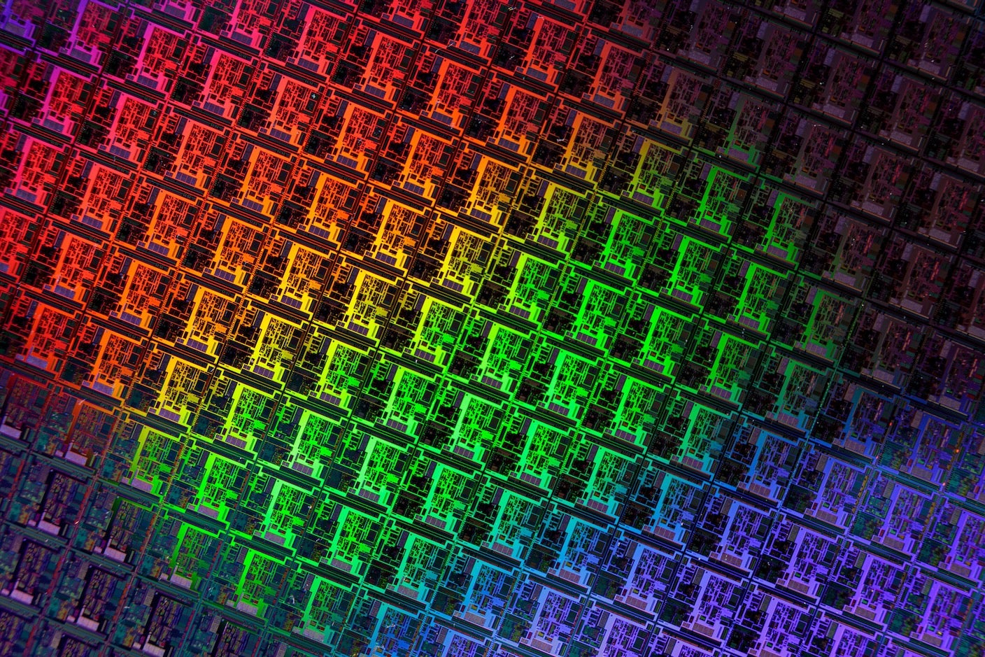
The relentless shrinking of silicon elements has led to exponential enhancements in chip efficiency, however we’re beginning to hit bodily limits. Now researchers have developed a method to combine supplies simply 10 atoms thick into typical chips.
For many years, speedy advances in miniaturization meant the variety of transistors on a microchip doubled roughly each two years, a phenomenon dubbed Moore’s regulation. However as these elements began reaching dimensions of only a few nanometers, progress began to stall.
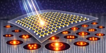
This left researchers and chip firms casting about for brand new methods to squeeze computing energy into ever smaller areas. So-called “2D supplies” are a promising method ahead. These crystalline constructions are only a few atoms thick and exhibit distinctive digital capabilities.
Up to now, it’s been difficult to combine such unique supplies into typical electronics. However now researchers at Fudan College in China have created a chip that mixes a reminiscence core product of the 2D materials molybdenum disulfide (MoS₂) with CMOS circuits.
“This work offers a promising technical pathway to convey promising 2D electronics ideas to real-world functions,” the authors write in a paper in regards to the new course of published in Nature.
The primary purpose it’s been laborious to mix 2D supplies and commonplace chips is that the tough floor of typical silicon circuits prevents them from adhering evenly and might injury their atomically skinny layers.
To get round this, the researchers developed a fabrication methodology they name ATOM2CHIP, which introduces an ultra-smooth glass layer between the 2D materials and the silicon. This offers each a mechanical buffer and a method to electrically isolate the MoS₂ layer from the electronics.
The staff used the brand new methodology to create a flash reminiscence array composed of a 10-atom-thick MoS₂ layer stacked on a 0.13-micrometer CMOS platform liable for transmitting directions to program, learn, and erase the reminiscence.
The chip might program bits in 20 nanoseconds and consumed simply 0.644 picojoules per bit—considerably much less power than typical flash reminiscence. An accelerated getting older check confirmed it might additionally retain knowledge for greater than 10 years at 55 levels Celsius. Programming accuracy was solely 93 %, which is nicely under what you’d anticipate from a business chip however nonetheless promising for an early prototype.
Kai Xu at King’s School London, told New Scientist the ultrathin design may assist resolve a long-standing downside in silicon electronics—sign leakage. Transistors work by utilizing a “gate” to regulate when present flows by means of a channel, however as they get smaller it’s simpler for present to slide by means of that barrier.
This implies they’re by no means actually off, which results in additional energy consumption and noise that may intrude with close by alerts. However the physics of 2D supplies imply transistors made with them have way more efficient gates, offering an virtually excellent on/off change.
“Silicon has already hit obstacles,” mentioned Xu. “The 2D materials may be capable of overcome these results. If it’s very skinny, the management on the gate could be extra even, could be extra excellent, so there’s much less leakage.”
One vital problem for the strategy is that the glass layer central to the method shouldn’t be but appropriate with commonplace fabrication traces. “This can be a very attention-grabbing know-how with big potential, however nonetheless a protracted method to go earlier than it’s commercially viable,” Steve Furber on the College of Manchester instructed New Scientist.
Nonetheless, the work means that if we need to kickstart Moore’s regulation, we could also be higher off abandoning the seek for ever smaller transistors and as an alternative give attention to ever thinner chips.


